
The next step is to create a shader for the board. Based on the textures previously set up, this decides where copper, soldermask or silkscreen should be visible and how these different materials should be rendered.
On GitHub we provide a sample project. There you can download the blender file, which contains a complete setup with models, corresponding textures and shader settings.
Integrating textures
First, the Shader Editor must be opened so that changes can be made to the material of the board. There, the previously imported textures can be added to the board's shader. The textures contain information about where soldermask, silkscreen or copper should be visible. All requirements for this were described in part 1.
A challenge now is to combine the textures in such a way that the textures of the top layer are only applied at the top and the textures of the bottom layer are only applied at the bottom. The geometry information of the mesh can be used for this distinction. The Shader Node Texture Coordinate provides the necessary vector information at the Generated output. These vectors contain values between 0.0 and 1.0 within the bounding box of the body. Considering only the Z coordinates of these vectors, a decider can be built using the Less Than node. This returns the value 0 if the Z coordinates are greater or equal to 0.5, that is from top to the center of the mesh. Otherwise the node will return 1 from the center to the bottom.
This decider serves as the Factor of a Mix node, which combines the top and bottom textures with each other. It has to be taken into account that the textures may require different UV maps. The screenshot shows the described arrangement of the shader nodes and how the black and white textures are mapped onto the 3D body.
The mixing of the textures has to be repeated for the other two texture pairs in the same way. Finally, the Mix nodes produce three outputs, which are needed for the further decision logic. It is recommended to group these nodes. The final setup of the layer masks is shown in the screenshot below.
Materials
A circuit board is made up of various materials. In Blender, almost any material can be represented using the Principled BSDF shader. This shader has a variety of parameters that need to be set accordingly. The values described here serve as a recommendation and are the result of trial and error. This means that depending on your needs, these parameters can also be varied to achieve better results. To better understand how the Principled BSDF shader works, the extensive Youtube video How to make Photorealistic Materials in Blender, using the Principled Shader from Blender Guru is extremely helpful!
In the screenshots below, the shader nodes for the individual materials have been grouped together. This improves the readability, especially when the materials need to be combined in the end (see section "Combining materials").
Silkscreen
The material of the silkscreen is the easiest to implement. It's Base Color is almost always white (#FFFFFF). Only the Roughness parameter has to be adjusted.
Principled BSDF parameters:
- Roughness: 0.9
Soldermask
The soldermask material has a special property. Since it is transparent, the soldermask appears to be brighter when there is copper underneath it. In order to consider this, it is best to manipulate the Base Color using the copper mask. This means that two colors, e.g. a light blue and a dark blue, are combined using a Mix node (see screenshot below).
Because the material is lacquer-like, we also experimented with the Clearcoat parameters of the Principled BSDF shader to achieve realistic light reflections.
Principled BSDF parameters:
- Base Color: #116CC2 and #053059 (blue soldermask)
- Roughness: 0.6
- Clearcoat: 0.4
- Clearcoat Roughness: 0.15
Copper
The copper refers to the exposed pads of the PCB. This is a metallic material that usually has a silver-ish or gold-ish color based on the surface finish used.
The surface characteristics can be controlled via the Roughness parameter. A value of 0.0 leads to a perfect metal surface that reflects light completely - similar to a mirror. However, this looks very unrealistic. Due to impurities or oxidation, the light reflection of the copper is much more diffuse. We felt that a value of 0.4 was appropriate.
Principled BSDF parameters:
- Base Color: #FFDF7F (gold-ish) oder #E9ECF2 (silver-ish)
- Metallic: 1.0
- Roughness: 0.4
- Specular Tint: 1.0
Base material
The base material of a circuit board can primarily be seen on the side. It consists of a glass fiber compound and is therefore slightly transparent. For this it is suitable to adjust the Transmission parameter.
Additionaly, this material has a layer-like structure. This can be implemented with the help of a Checker Texture. This texture alternates between two desaturated shades of brown in Z direction. The configuration of the Checker Texture is shown in the screenshot.
Principled BSDF parameters:
- Roughness: 0.8
- Transmission: 0.3
Decision logic
Now that all materials have been set up, they must be combined with each other using a certain logic. The black and white textures of the copper, soldermask and silkscreen layers (layer masks) serve as the basis for the decision making. The following assumptions are made:
- In case of the copper mask, white represents no copper while black represents copper.
- In case of the silkscreen mask, white represents no silkscreen while black represents silkscreen.
- In case of the soldermask mask, white represents soldermask while black represents no soldermask.
Combining materials
The individual layers (copper, soldermask, silkscreen) are added to the base material of the board in a specific order. This results in a hierarchy which must be taken into account when combining the materials.
-
The bottommost layers are the base material and the copper layer. The copper mask is used to decide where copper should be visible. If no copper is present, the base material is selected.
-
Above this is the soldermask. Wherever there is soldermask, the copper material and the base material should not be visible. However, there is one exception: the soldermask may only be present on the top or bottom. In other words, either copper or the base material is visible in holes or in the intermediate layer (which is considered by 2*).
-
At last there is silkscreen which "overwrites" all other materials below. The silkscreen mask is used to determine where the it should be visible.
When combining the soldermask and the base material, another decider comes into play (called "Middle Decider" in the screenshot). It returns the value 1 if it is the top or bottom layer and 0 in between. Using a ColorRamp and the Z coordinates of the Texture Coordinate node, a mask texture can be generated where black stands for 0 and white for 1.
Calculating Displacement
With the help of displacement, the surface of a body can be deformed. This makes it possible to display the height differences between the individual layers. The layer masks can be weighted with a coefficient and summed up. This can be done by a dot product of two vectors in the Shader Editor (see screenshot). The resulting value corresponds to the magnitude of displacement.
The second vector contains the weights 30, 30 and 14. At the end the dot product is scaled down by 0.001 using a Multiply node, so that the deformation is not too strong. In short, the displacement is calculated by this formula:
Displacement = 0.001 * (30 * CopperMask + 30 * SoldermaskMask + 14 * SilkscreenMask)
When calculating the displacement, make sure that the copper and silkscreen mask are inverted so that they add up correctly.
Final setup
Once everything is properly connected, the shader for the board should look something like this:
Summary
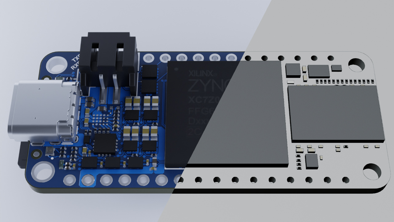
The 3D model of the board has now been equipped with a complex shader. This shader is able to mix different materials, so that they are displayed in the places as specified by the layer masks. Also, a displacement was added to the material, which shows the height differences of the individual layers.
Next part: Rendering PCBs (Part 3) - Final steps