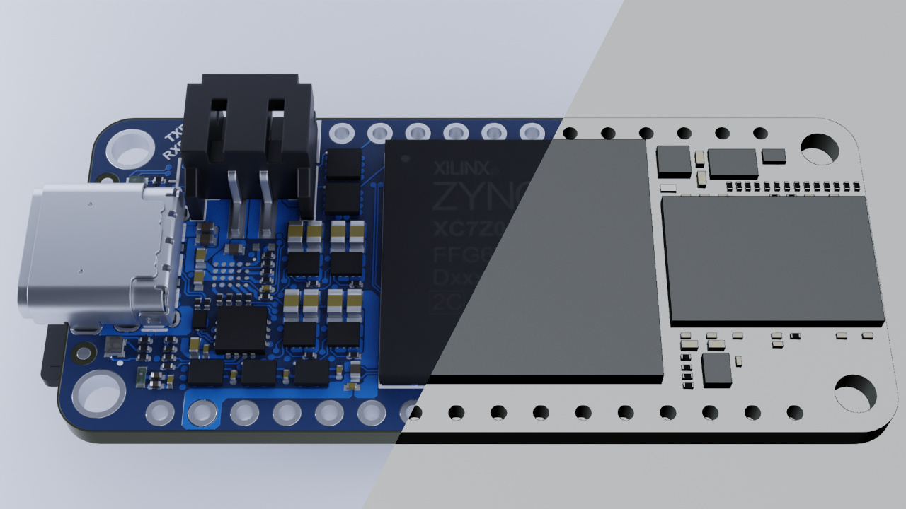

In this tutorial series we would like to explain the procedure of creating realistic renders from 3D models of PCBs in Blender. The first part covers the preparation of the 3D objects, the required textures and UV unwrapping.
On GitHub we provide a sample project. There you can download the blender file, which contains a complete setup with models, corresponding textures and shader settings.
Preparation
The most important thing is of course the 3D model of the PCB. Additionaly, the components placed on it can also be imported. However, these will only be considered in part 3. To import the models into Blender, the board must first be exported from the CAD program in which it was designed. This depends on which program you are using. In our case we exported .step files from Altium and converted them to a .obj file and associated .mtl file using the free tool DesignSpark Mechanical.
After importing the 3D objects into Blender, it is recommended to clean things up. This means simplifying the geometry of the objects, merging objects that belong together and grouping components using collections. This makes it easier to work with the objects and it also improves Blender's performance. These steps are explained in more detail below.
Merging Objects (Join)
Sometimes it happens that single components consist of many small pieces. An example is the USB-C connector shown in the screenshot, which consists of about 1000 objects.
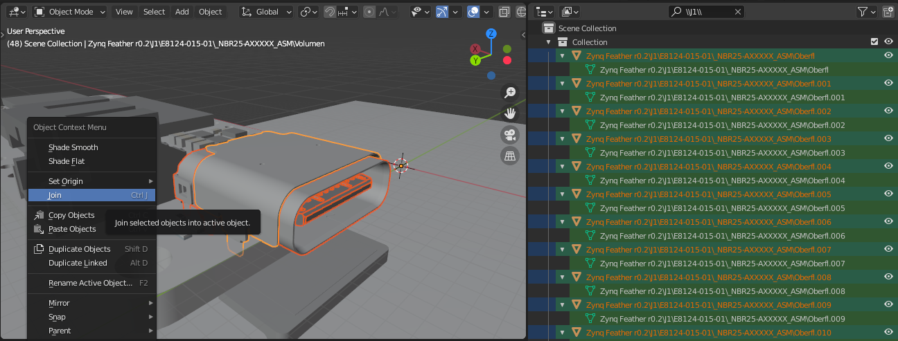
In order to simplify this complex geometry, all individual pieces must be merged into one object. To avoid having to tediously select all the individual parts, it is worth using the search function in the Outliner. In the screenshot you can see that the identifier J1 was used and therefore all objects that belong to the component J1 are shown in the Outliner. Then you can select all filtered objects using A and join them using Ctrl + J in the Viewport. It is important that one object is highlighted in yellow.
Simplifying the geometry (Limited Dissolve)
In Blender there is a convenient method to simplify meshes using the Limited Dissolve method. The detailed USB-C connector can serve as an example again. It has 31824 faces after joining all pieces together and is thus quite complex!
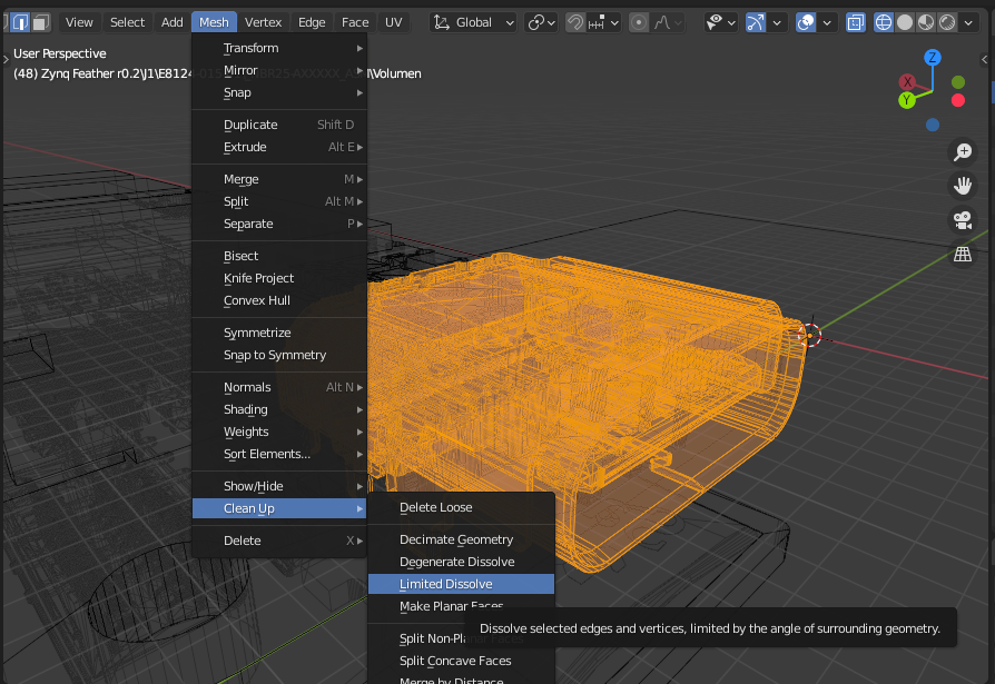
In the Viewport, the Limited Dissolve operation can be accessed via the menu Mesh > Clean Up > Limited Dissolve. After the simplification, the USB-C connector has only 6639 faces. The geometric complexity could be reduced significantly (by 79%)!
Using Limited Dissolve is also beneficial for the board, which can have quite a lot of edges and faces due to holes or vias. For small components or ICs, this method usually does not bring any notable improvements.
Grouping objects in collections (Move to Collection)
This step is optional and only serves to organize the objects in the Outliner. Similar to merging objects, it is recommended to search for components by their identifier. For example, in the screenshot we filtered for capacitors using the search pattern \\C[0-9] (meaning that the name of the object should have a "C" after the backslash followed by a number between 0 and 9).
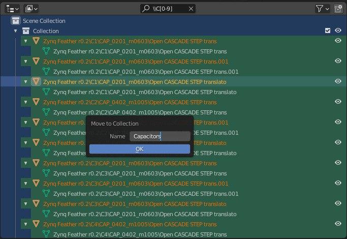
After entering a suitable search pattern, you can select all filtered objects with A and call the Move to Collection menu with M. There you can decide whether the selected objects should be moved to an existing or a new collection. In the example shown here, a new collection is created with the name "Capacitors".
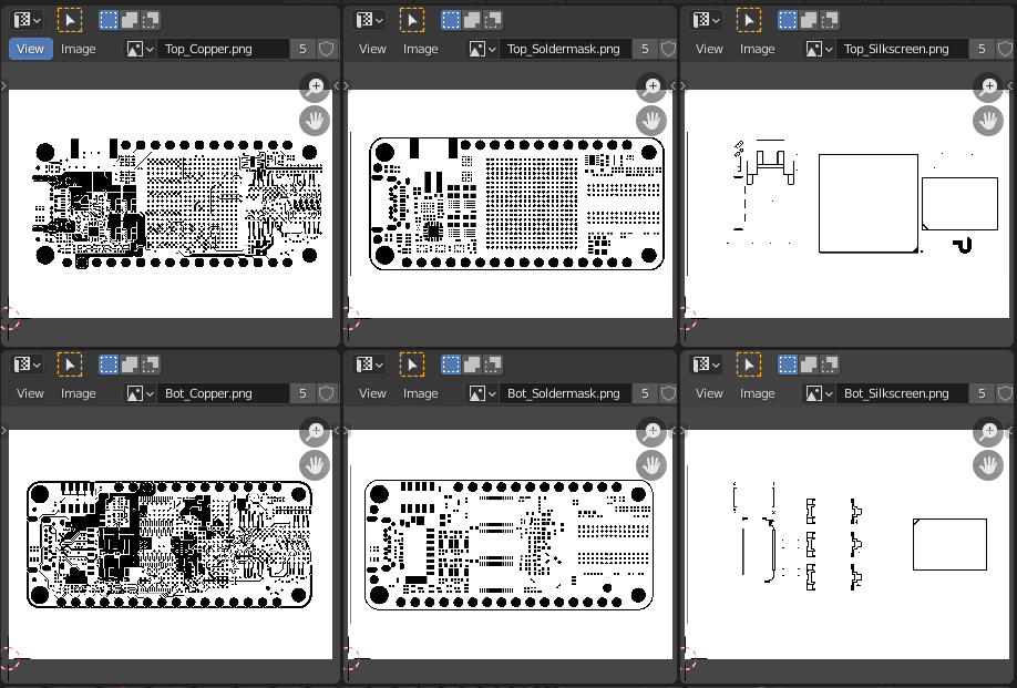
Textures
Different textures are needed to render traces or the solder mask on the 3D model of the PCB. These textures are black and white images generated by the CAD program. The following images are needed:
- Copper Layer
- Silkscreen Layer
- Soldermask Layer
If both sides should be taken into account, different textures are needed for top and bottom. In this case, you need six textures for the board.
In our example project, we have chosen a resolution of about 4600 x 3300 pixels (be generous here) for the PCB textures. The export of the images may vary depending on the CAD software. If the CAD program does not allow a direct export of PNG images, one possible solution is to export the layers as vector graphics or PDF and then open them in GIMP. There the image can be cropped and saved as a PNG image.
In Blender image files can be opened in the UV Editor. Three or six textures should now be present (see screenshot).
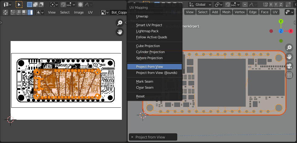
UV Unwrapping
In UV Unwrapping, two-dimensional textures are assigned to the faces of a three-dimensional object. To project the textures onto the surface, you can use the Project from View method. Before the unwrapping is performed, it is important that the viewport has the top perspective. Numpad 7 can be used to switch to this perspective. In Edit-Mode open the UV Mapping menu using U and execute Project from View.
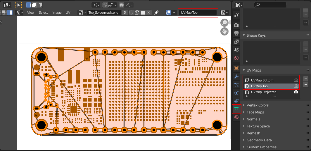
After unwrapping, you can see the projected geometry of the board in the UV Editor (left in the above screenshot). This now needs to be aligned with the textures. When aligning, make sure that all surfaces are selected (orange) both in the viewport and in the UV Editor so that everything is scaled and moved evenly. The holes and the outline of the board are useful for alignment.
It can happen that bottom and top layers are misaligned. If this is the case, two different UV Maps are required for the board object. UV Maps can be managed in the Properties window under Object Data > UV Maps and can be swapped in the UV Editor (see red boxes in the screenshot).
Summary
The 3D models and the textures are now prepared for the subsequent steps. In the next part, we will look at the configuration of the board's shader. Based on the textures, the shader decides where copper, solder mask or silkscreen are visible and how these different materials should be rendered.
Next part: Rendering PCBs (Part 2) - Shader Setup